Q1: Inferring Xilinx RAM's (Distributed or block), Single and dual port with different characteristics?
A: Below link provides details of all kinds of Xilinx RAM's. Also these are technology independent and XST (Xilinx synthesis tool) offers automatic RAM recognition capability.
http://www.xilinx.com/itp/xilinx4/data/docs/xst/hdlcode14.html
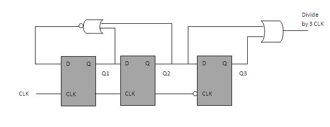
Q2: Generate a divide by 3 clock with 50% duty cycle ?
A: Below circuit will generate divide by 3 clock.

- output of flop 1 and 2, Q1 and Q2 is connected to NOR gate.
- output of NOR gate is fed back as input to flop 1.
- Q1 will be a divide by 3 clock without 50% duty cycle.
- Q2 is the registered version of divide by 3 clock.Also, Q1 and Q2 are sampled at the posedge of the reference clock.
- Q2 is fed to flop 3 and here the sampling will be done at the negedge of the reference clock.
- output of flop 2 and 3, Q2 and Q3 are connected to OR gate to generate divide by 3 clock with 50% duty cycle.
Below is the waveform explaining the clk-by-3 circuit:

Q3: Generate a divide by 2 clock and divide by 4 clock ?
A: Below circuit will divide the clock by 2:
 Q-bar of the flop will be fed back to the D-input of the flop,
thus generating divide by 2 clock at the output, Q
Waveform is as shown below:

Below circuit will divide the clock by 4:
 Q-bar of the second flop will be fed back to the D-input of the first flop,
thus generating divide by 4 clock at the output, Q2
Waveform is as shown below:

So, to generate any clock which is to be divided by powers of 2, we can add extra flops and take the Q-bar output and feed it to the D-input of the first flop.
A: Below link provides details of all kinds of Xilinx RAM's. Also these are technology independent and XST (Xilinx synthesis tool) offers automatic RAM recognition capability.
http://www.xilinx.com/itp/xilinx4/data/docs/xst/hdlcode14.html
Q2: Generate a divide by 3 clock with 50% duty cycle ?
A: Below circuit will generate divide by 3 clock.
- output of flop 1 and 2, Q1 and Q2 is connected to NOR gate.
- output of NOR gate is fed back as input to flop 1.
- Q1 will be a divide by 3 clock without 50% duty cycle.
- Q2 is the registered version of divide by 3 clock.Also, Q1 and Q2 are sampled at the posedge of the reference clock.
- Q2 is fed to flop 3 and here the sampling will be done at the negedge of the reference clock.
- output of flop 2 and 3, Q2 and Q3 are connected to OR gate to generate divide by 3 clock with 50% duty cycle.
Below is the waveform explaining the clk-by-3 circuit:

Q3: Generate a divide by 2 clock and divide by 4 clock ?
A: Below circuit will divide the clock by 2:

thus generating divide by 2 clock at the output, Q
Waveform is as shown below:
Below circuit will divide the clock by 4:

thus generating divide by 4 clock at the output, Q2
Waveform is as shown below:

So, to generate any clock which is to be divided by powers of 2, we can add extra flops and take the Q-bar output and feed it to the D-input of the first flop.


